Project
Projecttitel: TTSH rev3 buidling guide
Status: FINISHED
Startdate: 21.Dec.2016
Duedate: 31.Dec.2016
update 12.Jan.2017 Mouser Link updated
last update 13.Jan. 2017 Major bug found
Manufacture link: http://thehumancomparator.net/
due to changes in my webhosting (rootserver) costs for RAM/Backup and my worktime in Adminstration of the Server & Web Application Server it would be very helpful to use my paypal gift function, thank you
This guide is complete yet ( last update on 12.Jan.2017)
please check my rev.2 build guide and hardcorebuildguide, gatebooster pages, that gives you more infos and knowledge.
the TTSH project isn`t for beginners !
Feel free to register a account for free, you can comment, export pages, you stay informed with pageupdates by email.
send me a message if you want edit my pages, i´m looking for supporters.
further i´m looking for authors too, please contact me
Table of Contents
open tasks:
- LED-man add a trusted builder list (please contact me if you want listed here as trusted builder)
Trusted Builders:
| Name | Region | Contact | |
|---|---|---|---|
| Fuzzbass | USA | fuzzbass "at" verizon.net | |
| Elmigel | USA | Pete.hartman "at" gmail.com | |
| Dave.H | USA | ishkabbible "at" gmail.com | |
| LED-man | Europe/worldwide | check my Impressum |
BOM: (Bill of material)
The shared mouser basket from thehumancomparator is wrong (22.Dec.2016)
(this Mouser basket was provided in the 'order' eMail)
https://www.mouser.de/ProjectManager/ProjectDetail.aspx?AccessID=234c0 9ed60 old link from JON
http://www.mouser.com/ProjectManager/ProjectDetail.aspx?AccessID=6CEDD31990 new link from me, improved see notice field for quantity "order 10"
order the 100K resistors, 2N3906, 2N3904, 1N4148 from a local dealer to save money, make sure the 2N3904/2N3904 is from tape - for better transistor value matching.
dont miss to order the parts for the gatebooster too.
delete the following parts from your mouser basket: 652-SRN6028-101M 710-744290321 these chokes/filters aren´t needed in rev.3
Printable BOM as listed, (rev.2 plus additional list for filter and psu)
ttshv2BOM.pdf (mainboard pcb) - i update the list in next 2 days. (remove the above listed SMT chokes and replace with chokes from SecondFilter_BOM)
4027v2BOM.pdf (vco boards)
TTSHrev3_SecondFilter_BOMv1.1.pdf (filter board) please use matched pairs 4 pairs of 2N5087 and only matched pairs for 2N3906/2N3904 (exept the single trannys)
for the rare parts, please check thonk.co.uk
if you need matched pair trannys or single tested trannys like 2N3954/8 or others, please contact me.
further i offer a survival kit
(link to my rare parts/survival page)
dont miss to order:
Speakers: Visaton SC8 (reichelt.de, tme.eu)
reverb tank https://www.banzaimusic.com/Belton-RBL2AB3C1B.html see known issues for wiring
RCA/Chinch cable 0,5m - 1m (double or triple isolated otherwise you gets hum issues)
DC Powersupply 24V/1A DC (preferred, 12V - 24V works) middle pin is + (5,5mm/2,1mm size)
Cable for Power wiring and Speaker wiring (for power ist required the usage of minimum 1mm² diameter )
13 x 12mm Spacer M3, black flat Screws for fronpanel, screws for speaker at the rear and spacermounting, washers, nuts, cable shrink, silicon for matched pairs or glue the trannys together
3x long spacers to mount the powersupply (30mm-50mm preferred to minimize the risk of EMV issues )
as stated above, the project isn´t for beginners
nearly all professional builders have standard resistor and capacitor values at home (if the BOM miss a few standard parts like a 100K resistor)
known issues:
- Major Bug: Description: at the Frontpanel pcb side you find some "VIAs", at the VCO 3 section the jack S/H has a via with 15V, the metalcase of the jack is connected to ground and you run in a short between ground from the jack and 15V from the via, there are 2-4 other jacks with vias too (i report asap all related jacks today evening)
Solution file down the jack at the position of the via (1mm is fine)
- Improvement: Powersupply Board - turn the 2pol MTA156 header if needed - otherwise the power input cable is above the powersupply.
 confirmed
 - Minor Bug:Main board – Missing trace from V- to header. (copyright of picture for thehumancomparator.net ) confirmed

- Minor Bug: 4072 VCF missing trace pin 4 on LM1458 to -14V (use shrink tube for isolation) confirmed

- Minor Bug: 4012 VCF Board — BC558 must be installed backwards, schematics show Ermitter to 23k2 resistor in rev.7.2 (v2) confirmed

- Minor Bug: for all 2N3958 and 2N3954 change 2 pins like this, cross the both pins - use shrink tubing for one pin for isolation. confirmed

- Improvement for build: or the Filtercards use flat electrolyte capacitors, check the hight of all parts - if needed use other headers, check this for both Filtercards before you solder the headers, if needed place the 47pf(50pf) MLCC capacitor (on the mainboard) on solderside of the pcb)
on my first build i used a 10mm spacer but i prefer the usage of 12mm spacers, (by usage of 2 spacers - its needed to cut on the VCF out jack at the bottom some metal and you need a flat screw, in result one spacer is enough )
)
- Minor Bug: by usage of the banzai reverb tank, run in the reverb tabk a wire from ground to ground on the RCA connectors to ground output and input
Minor Bug: turn 180degrees on the mainboard the 5pol MTA156 powerheader, otherwise the powercable is to the wrong side.
Tips:
use 3x 20k or 25k multiturn trimmer Bourns Trimmer 3296Y-1-203LF (Y footprint instead of W, W fits to with bending the legs ) for V/OCT trimmer in the VCOs, but this must mount from the pcb parts side (not the same side as the frontpanel), you must calibrate the VCOs from rear side, but its more accurate to calibrate as with single turn trimmer
buildguide:
This guide is for users with experience in SDIY, you need a scope and a frequency counter, DMM/DVM/LCR-Meter)
i dont share infos about polarity of capacitors, this basics skills are required, otherwise feel free to ask me for a assembly service. (check the trusted builder list)
please use a fume extractor.
its needed to solder 6 SMT caps in 0805 format and 2 SMT power regulators.
this guide is a best practice guide, i´m not responsible for failures/malfunctions/defects.
- lets start with the powersupply board - add all needed parts on the pcb, start with the two SMT power regulators.
there is one missing part (a dual choke) - please use wire links here or resistor legs
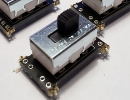
turn the 2 pol MTA header as described in the picture
if needed - wash the pcb carfully on the solderside
testing/trimming: use a 18-24V DC powersupply for input and set the output to 15V/-15V by usage of the both trimmers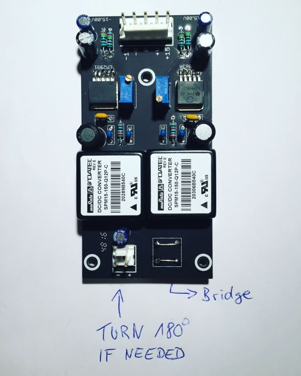
- Mainboard PCB - place all IC-Sockets ( tin one ic socket from top, place the ic socket and heat the ic socket pin - the socket drop in place
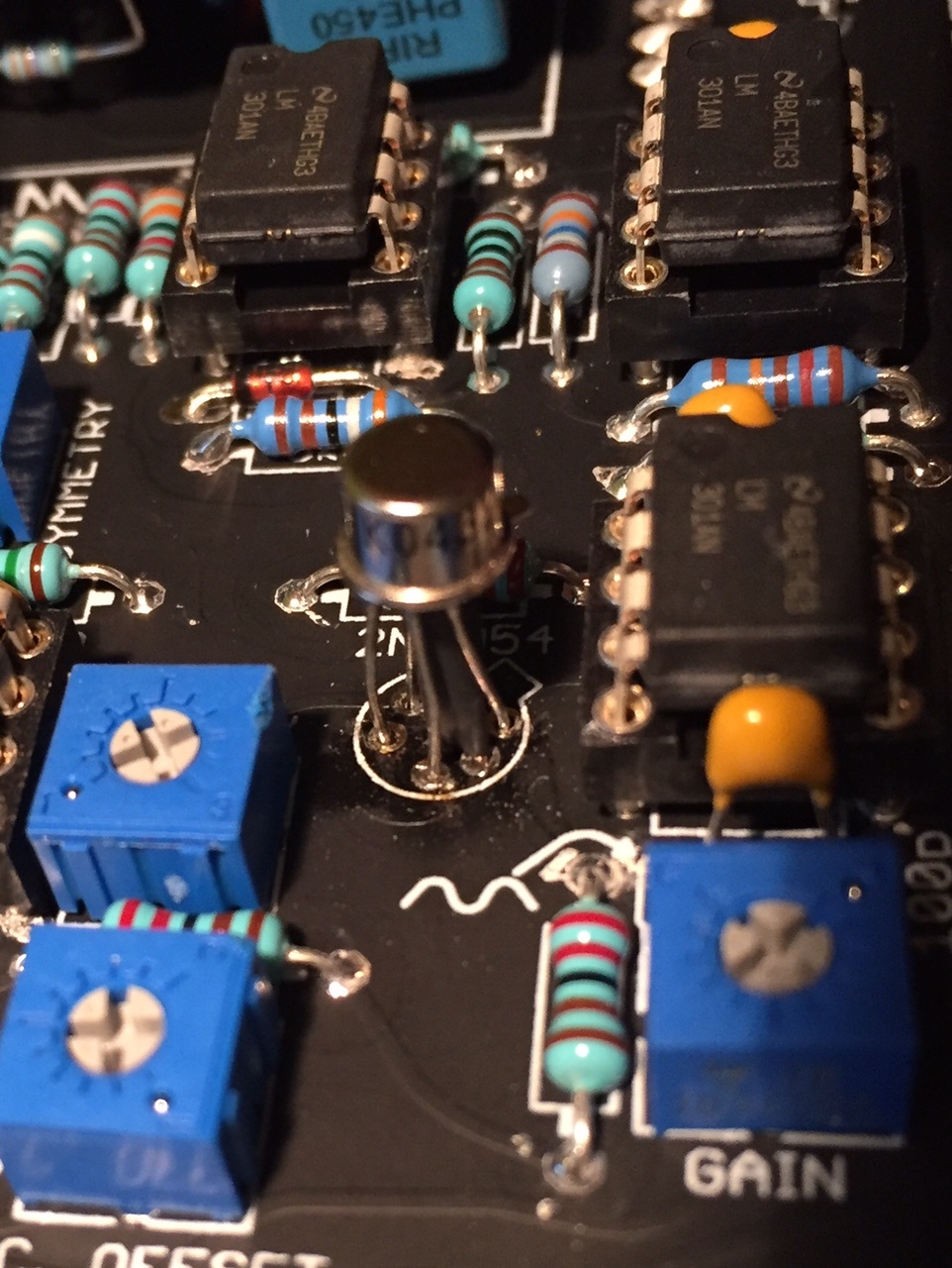
on the rear side of the PCB is for the LED driver a ic socket - we dont use this one - dont solder a ic-socket here ! see step14 - best practise - begin with the "most use values" and end with the value range Mainboard PCB - start with 100K resistors, 10K, 1K, 1M, 100R (reverb), 10R (Amp) 10M (top right)
if done - 47k, 4k7, 470K, 4M7, – 22K, 220K, 220R, 2M2, 33K, 3M3, 330K... — 30K1, 680R, 68K, 68K1, 680K... ..... and all other
please remember: on solderside are few resistors too - on VCO 4027 boards and filter boards too - its your choice to leave it for later or assembly it yet too (i prefer later) - Mainboard PCB - place all rectifiers 1N4148
- solder from top all parts
- cut the resistor and rectifier legs from bottom side
- place all MLCC caps and solder from top
- place all polyester/polypropylen caps - bend the legs from top
- add all transistors in place and solder one pin from top -(except the 2N3954, both 2N3958 - if you cant test this, use a milled IC-socket and cut the pins out - use this as socket)
- turn the pcb and solder all pins. (no switches, no fader, no jacks, no pot, no trimmers)
- you find on solderside few resistors - but take a look at step 14 - you don´t need the 3 resistors for the LED driver ( LEDs works too)
- wash the pcb 2-3 times if needed, i use Ispopropylen alcohole
- make a breaktime/pause yet - the pcb needs time to dry - if you dont need a breaktime/pause - assembly the filterboards and 3 VCO 4027 boards - wash the pcbs too, make sure you use flat 10uF electrolyt capacitors, use c0g, polypropylen or silvamica for the 680pF cap, don`t mount the connectionsheaders yet
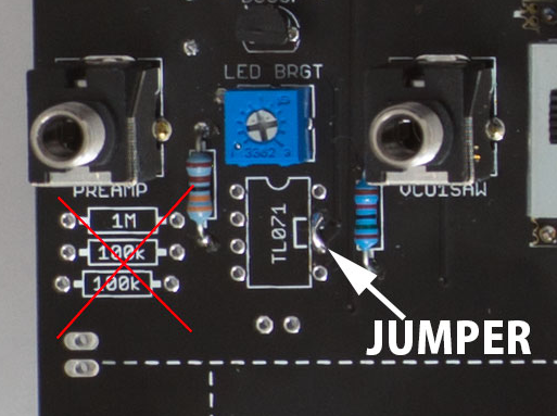
- on the PCB solder side, there is ic socket for the LED driver (near the multiples) its needed to bridge with a resistorleg the middle pins
- Mainboard pcb: its time to add all other parts on the pcb - i prefer multiturn trimmers for the VCO V/oct trimmers 20K or 25K, but remember this can´t mounted on the frontpanel pcb side due to sizing, you have to open your TTSH for trimming the VCOs, begin with trimmers, faders - for faders keep attention on correct pcb side, best practise for faders: turn the pcb upwards on your desk add 4 faders in place, one hand holds the faders with other hand bend the faderpins with a flat screwdriver, solder all faders, add the Gain pot on top and solder them.
- add the header/sockets for VCOs, Filtercard - best practise: mount each header in socket - put them in place on the pcb - add the vco pcb on top and solder at first on top (sub vco pcb to header) not the header to mainboard pcb.
then start the soldertask for the other side. - check on your pcb other parts: you need to assembly few 2pol, 5pol MTA headers (gate/trigger/power) solder in the RCA jack for reverb, you have to add a 3 pol MTA header to powering the optional Gatebooster and/or TTSH sync board , on each section you find 6 pol holes.
- now its nearly done - doublecheck all solderpoints, missing resistors,caps..
- add the 13x 12mm spacers for speaker to pcb, dont fix it very strong - we need to align this in step 22
- you find on the pcb on left bottom near the speaker hole switch adapter pcbs, cut them out and place they behind the switches
- setup all 81jacks in place, don`t solder the jacks yet
- place the frontpanel on the pcb/spacers - fix it with screws - if needed align the spacers
- add on each corner a washer and nut to a jack and at the bottom/near of the voltageprocessor
- at this time you need four hands if possible.. to turn the pcb without loosing jacks
- solder at first the jacks from step 21
- check the switch posistions, align it and solder 1-2 pins (middle pins), check again the positions, if needed correct it.
- if the alignment of all parts are fine, solder all swicthes and jacks
- if needed clean with eartips and isopropylen the solderpoints of silder/switches/jacks
- add the 3 VCO 4027 modules and one filtercard in place.
- time for wiring: speakerwiring/headphone,
- Wire first to headphone jack, then to speaker.For the left amp :Connect pad L to tip pin, connect switching tip pin to left speaker. Connect GND pad to speaker.For the right amp :Connect pad R to ring pin, connect switching ring pin to right speaker. Connect GND pad to speaker.And finally connect sleeve pin on jack to ground somewhere on board. (external gate ground is good choice)So when headphone is inserted it breaks the connection to the speakers.
- unmount the panel, add 3 long spacers (20-50mm to the 3 holes near voltage processor - the stands are used for the powersupply yet - mount the psu pcb on top), remount the panel
- wire the powerswitch between + line and the powersupply pcb input
- for power between powersupply and mainbaord - doublecheck the polarity,
- testing and trimming later here or check http://thehumancomparator.net/wordpress/instructions-ttsh-trimming-instructions/
Gallery
| There are no images attached to this page. |
Stats