Alll Users who have access on this page also have permissions to EDIT this page, feel free to add new issues/tipps or improve this page.
(the page have a page history and version control, don´t by shy to edit this page)
PLEASE support my pages to cover my Server fees
Updated: 19.dec.2019 Patrick.J aka DSL-man
updated: 10.March 2020
DO NOT SHARE THIS INFOS in public domain - its copyrighted (by Matthias and me), thank you.
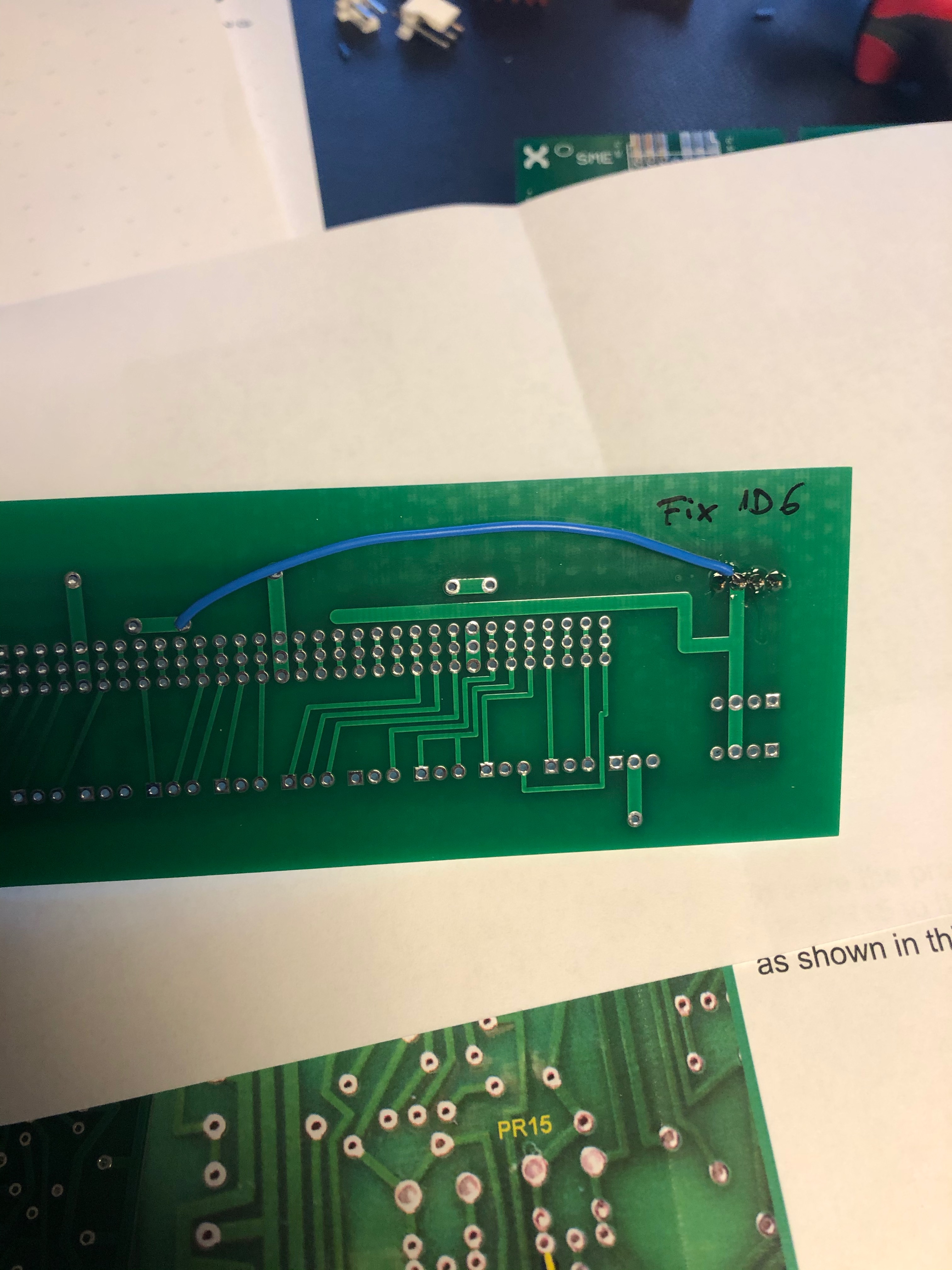
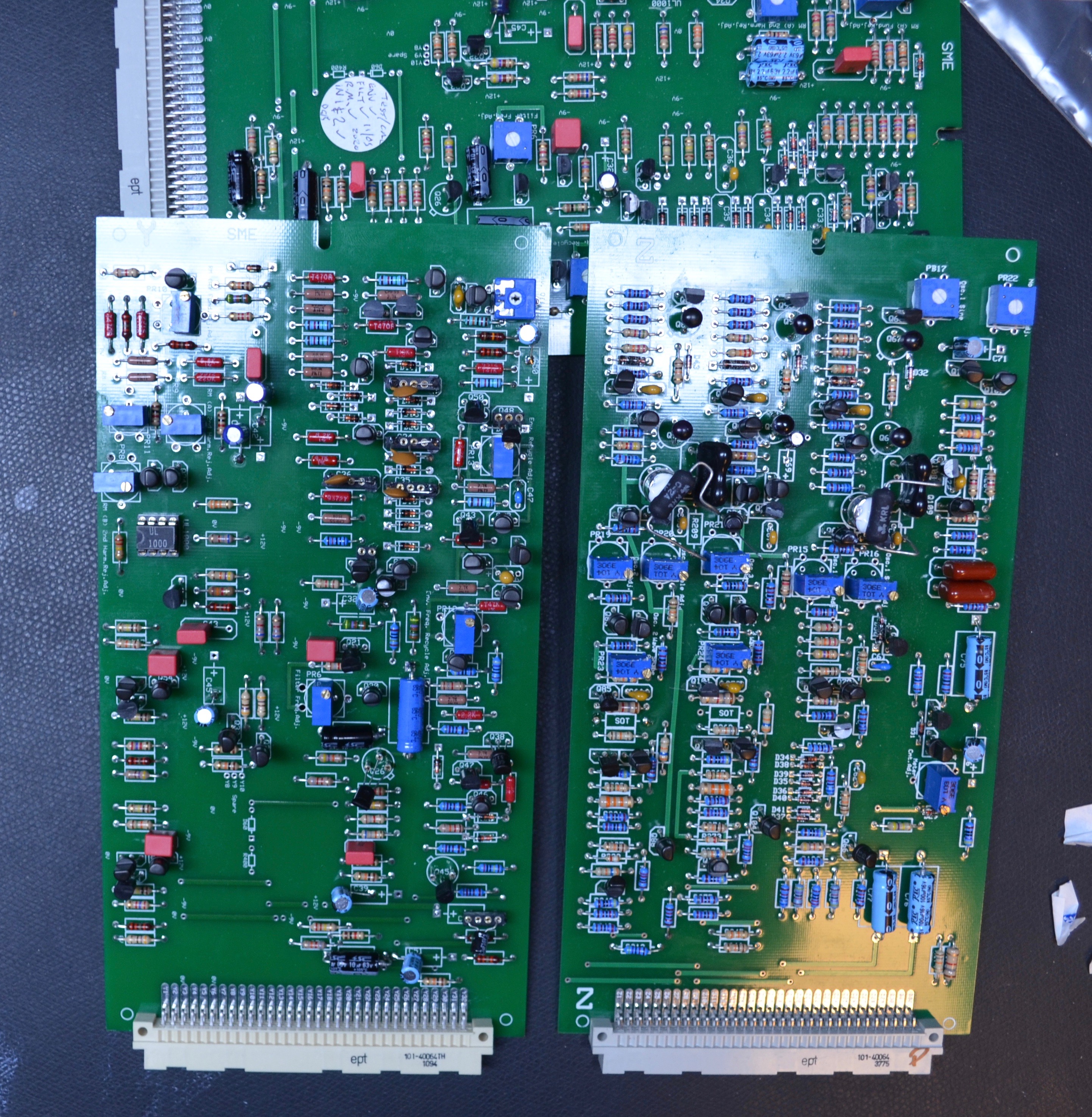
for all Cloney Users who have the PCB Version Z17/10 mk4 cba SME (from 2017/18) please use this link : The Cloney - secret files
important is the issue on the Z card or you short -9 and 12V
the latest Version is Z19/09 Mk4 cba (you find it on rear of the Z card) for this is following issue list except my build tips which are for all versions
ID
MatthiasIssueNr.
Issue release date
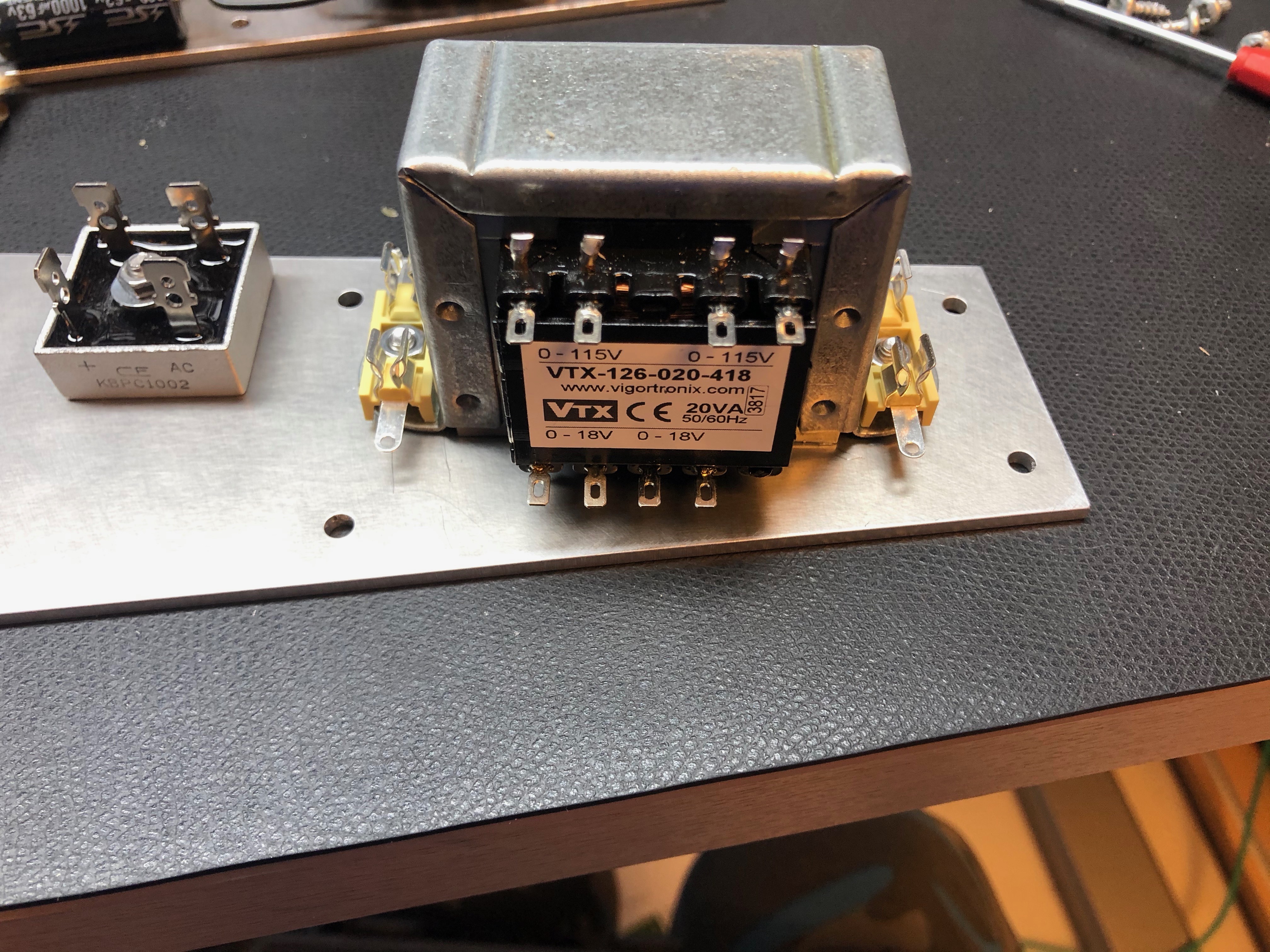
Issue
Solution
1
29
19.dec.2019
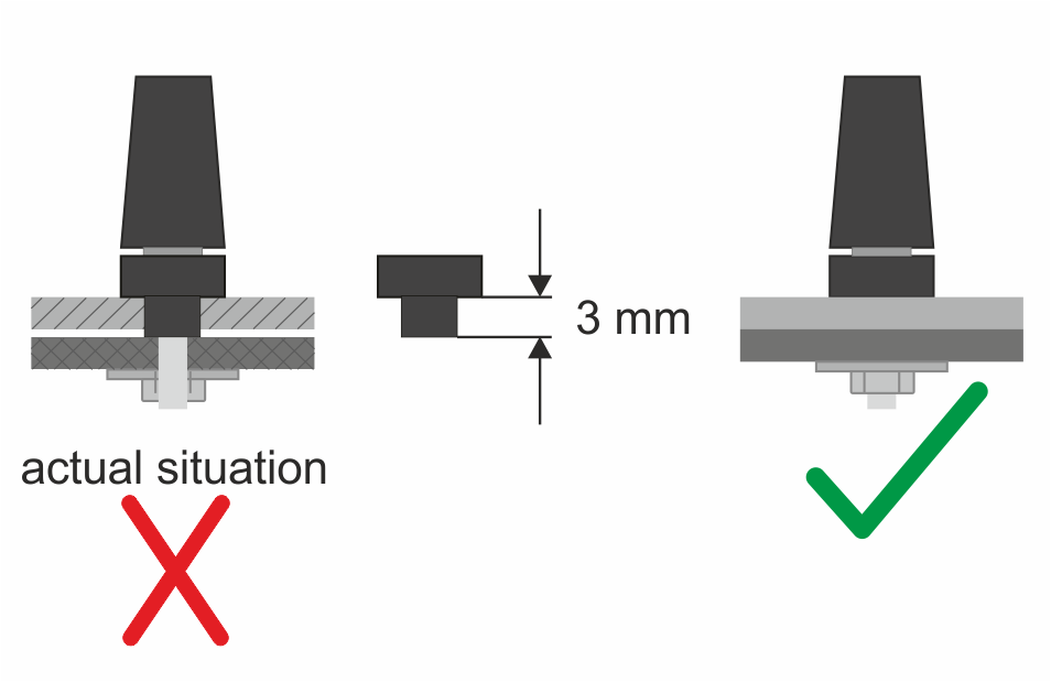
When mounting the matrix to the lower frontpanel by the ground terminals, a distance of 1 - 1.5 mm can be noticed between the matrix's surface and the frontpanel. Caused by the production charge of the ground terminals. In this charge the isolating upper bushing of the terminal is longer than usual. See the attached graphic therefor.
File down the narrow part of the bushing to at least 3 mm or less. Use a file or some sandpaper, a countersink will also help. Another option is to re-drill the matrix at these two holes to the diameter of 8.6 mm.
Plan B: try a washer or 2 of them (not tested yet)
Plan C: Re-drill the matrix at these two holes to the diameter of 8 mm and file down the tooth.
2
28
16.dec.2019
At the Z board there is a link missing on the 12 V trace. See the attached photo
The failure affects OSC 1..
3
27
16.dec2019
At the Z board the captions of the presets are not printed.
See herefor the attached page of the population guide.
4
26
08.dec2019
"I meanwhile realized the EK construction manual gives no detailled information about mounting the matrix to the lower panel. So I decided to extend the manual by an additional page.
Find this new page attached to this Newsletter.
With this change, the actual EK construction manual now is rev. 1.24 and will be part of the next shipments (serial 078, 101, 106)."
5
25
04.dec.2019
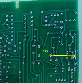
PCB Version: Y19/09/mk4 cba
There is no trace error at the X board.
It is at the Y board - I am sorry.
As reported, it was already soldered by Derek before packing the Electronics-Kit. But its good to check this one more time, as the soldered wire can be fallen off whilst transportation or handling.
Therefor see the attached photo. If this link is not present, solder a piece of wire to complete the trace.
6
24
03.dec.2019
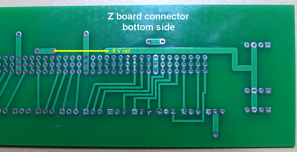
There is a track error at the -9 V rail. Its at the bottom of the Z board area in the BACKPLANE !!
See the attached backplane photo.
Solution: Solder a cable as shown in the picture (yellow link) to connect the right part of the -9 V rail. The upper panel is usually connected to the power rails by one of the 4-pin sockets in this area.
7
22
03.dec 2019
Info only: Please refer to page 2 of the Population-Guide Version 1.92
Info: the 1K 2Watt resistor for the X board is for the PSU wiring... not on the X board pcb
use 1% metal film resistors or select the 2% resistors on board X.
9
Issue 30
27.dec 2019
R 12 (PSU / earth link) The wiring diagrams were not correct since an update earlier. This causes a parasitic voltage and in some cases obviously a strange behaviour
Solution: Exchange the specific pages at your manual by the updated pages attached to this newsletter and follow these instructions.
So the next shipments will include construction manual rev. 1.26 or even a higher revision.
howto for X card remove the Pin 4 and 8 (the connector for the 2 TIp3055)
11
Patrick
Early 2020
use a 7mm drill that the flat screws fits flat on bottom of the PSU base plate, only as seen on the picture on right side.
wide also the fuse holders with a 4mm drill that the delivered screws from the kit will fit thru the fuse holders.
12
31
Early 2020
Major Problem: At 110 - 120 V mains voltage, the primary wiring of the 115 V transformer causes problems on the secondary coils/outputs
Solution: Change the primary transformer wiring to the way, shown in the diagram attached to this Newsletter.
13
Patrick Issue
Summer 2020
Problem:
the regulators are too hot for my experience - we waste too much energy in heat
the 18V AC transformer is "wrong" here - we have a 27V DC output after the bridge rectifier, beer we only need 15V DC.
so I tried a 12V AC transformer which gives you a stable 18V DC output under load which is much better, the heatsinks are only at 22-30 degrees instead of 50C or higher.
TME PART number:
TS20/023
please note: you have to drill 3 holes in the PSU back plate to mount this.
14
Patricks
Summer 2020
Problem:
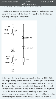
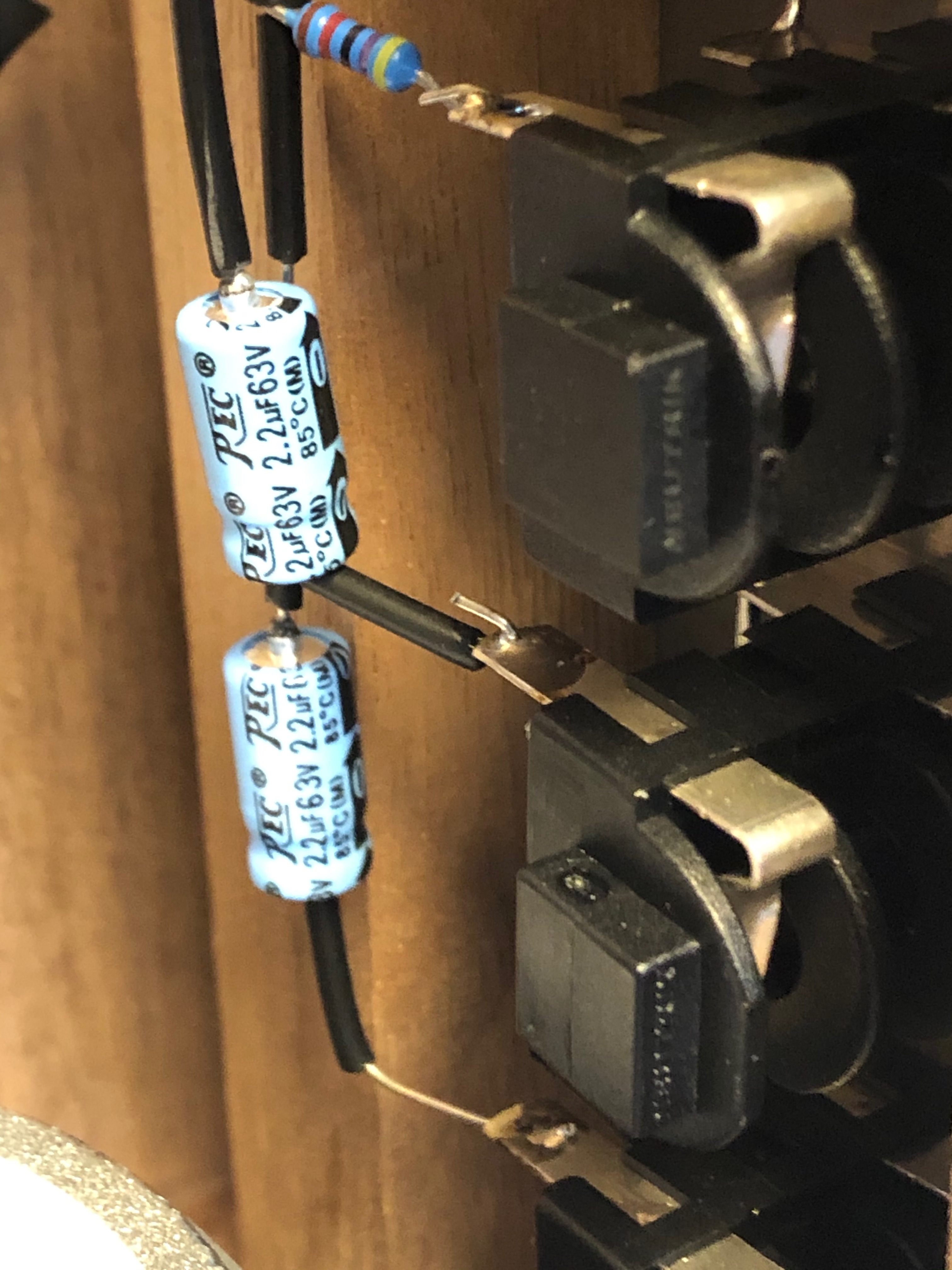
Envelope bleeds in VCOs
the Lamp is the root cause.
it can be replaced by a LED (preferred yellow)
you also Need a 6V8 zener (6.8V zener Diode and cable tube/shrink)
it was tested by me and works fine.
TME Led holder with included LED:
2658.8073 (mentor vendor part nr.)
6v8 zener diode: BZX55C6V8-TAP
15
Patrick
07/2020
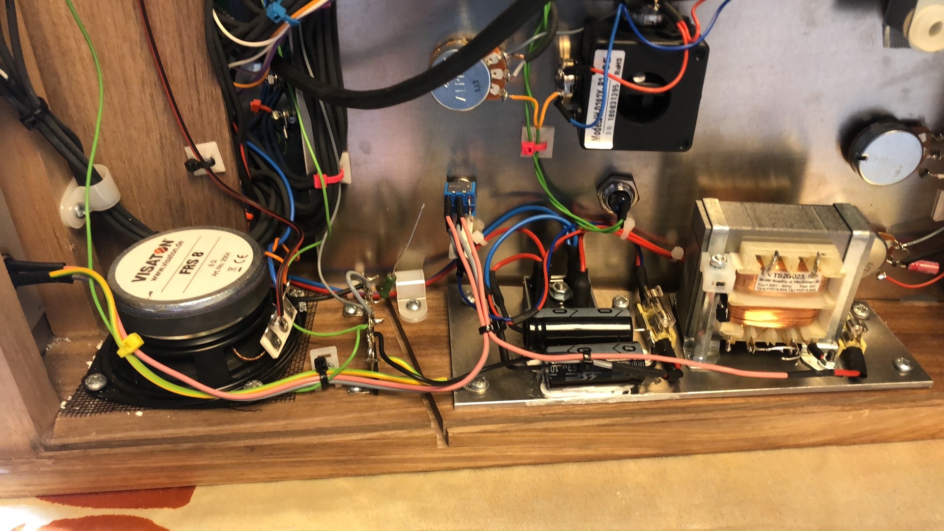
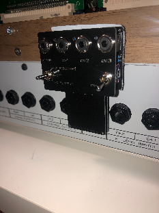
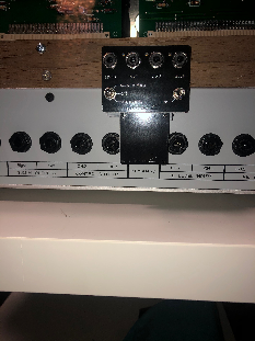
improvement: Buffer
see bottom picture
Paps offer buffer pcbs.. which means there's no voltage drop for the CV or Audio signal when you patch multiple sources and destinations ( 2x joystick to all VCOs Freq. for example)
some Parts from Reichelt (I don't have a full list)
Trimmer: 64W-100K
Diode: BZX 55C5V1 VIS (5.1 zener)
4x 3.5mm socket CLIFF FC681374V
2x NK236 Slideswitch
2x LM741CN
1x MKS2-50 680N. (680nf cap)
Calibration (the better Version)
Start with PSU, then Output Filter - the Output Filter
Click to expand:
Power Supply
Before turning on, set PR1 cw and PR2 ccw with only ‘A’ board plugged-in.
Set PR2 for +12V ± 0.1V Set PR1 for -9V ± 0.1V
Check PR2 again and reset if necessary
N.B. -9V rail is parasitic on the +12V supply.
Plug in ‘B’ and ‘C’ cards and recheck +12V and -9V rails.
These should not have altered. If they have, suspect either ‘B’ or ‘C’ board orpoor regulation on A board. Plug-in keyboard as extra load. +12 and -9 Volt rails should not have moved more than ± 0.1V measured always on the ‘A’ board. (‘C’ board voltage may be 20 mV lower)
Monitor the rails on the scope (5mV/cm). Look for hum and noise. These should be much less than 5mV. Noise, if present, will probably be due to the zener diode.
Power supplies should stabilise on full load for specified fluctuations.
110/240 nominal : +10% or -23%
110 nominal : 100V-135V for 125 sufficient
240 V nominal: 200V-260V
Hum can also be checked by the following:
Check Output Filters on 10 Output Controls on 10.0.10.10
Patchboard vacant
Monitor (5mV/cm) on signal output
Load unit with keyboard
100 Hz ripple as shown.
Noise can be seen which should never exceed lOmV p.p. Even with noise
level up. With noise level down, the noise on this waveform should be
quite low. Zener diode noise will be very obvious.
N.B. A2 normally gets hot, dodgy Dl gives large 100Hz ripple on Output. Always clean edge-connectors and check clean presets on ‘A’ board.
Click to expand: Output Filter:
Output Channels
Set Output Channel Filters to 5. Set Output Level row to 0.0.10.0 and connect traces of scope (5mV/cm)
to both signal outputs.
Connect full level ramp signal at 261 Hz from Oscillator 1 to both Outputs.Trim PR4 and PR5 for minimum signal breakthrough. (Maximum 5mv p.p) Replace presets if adjustment is erratic.
Reset Output Channel row controls to 5.0.10.5. Output levels should be around 1V p.p and should be within 20% of each other. Check signal tracking in thesame manner for Output settings 4 and 6 as well. If one level is consistently high, pad out resistor across its control pot (R305 = 56K)
Successful tracking will depend on the characteristics of the pots and the correct matching of the FET’s Q14 & Q18.
Connect the joystick row via two shorting pins to both VC level inputs. Swingstick up and down to check for 20% level tracking tolerance.(Level pots shouldbe at zero). Inaccuracies in stick tracking may be adjusted by altering thevalue of R302 or R304 (lOK) which are mounted under the patchboard rear.
Check correct operation of Pan controls, which only affect the Signal Outputs. Check also the Output Filters. Use noise as a good source.
Check for max. outputs on the Signal Output socket of at least 2.5V p.pbefore the onset of clipping. Level controls should be at about 6. Checkheadphone signal is good. Check for instability of Output Amps by driving hard with low frequency. (Oscillator 3 square wave). The level control of thechannel NOT being driven should be on zero. Monitor the two signal outputs.The undriven channel will show breakthrough. Plug in headphones and check for oscillation. Reduce drive to Output Channel 2. Keep checking for oscillation.Then repeat for other Output Channel.
N.B. DC offset across loudspeaker is 1.8V ± 10%.
Click to expand
Reverb
Reverberation
Set PR3 fully clockwise before operating. Feed large amplitude tone bursts into reverb. Adjust PR3 so that the output is dry at Mix setting of zero and reverberation progressively increases from setting of 2.
Maximum dryness on the Mix control should be no worse than thatobtained with the VC Mix input row on the patchboard grounded.
Check voltage control of Mix with the joystick.
Hold input amplitude constant and sweep frequency of tone. Check for rattles, buzzes or abnormal resonances in the spring. Check spring is correct way round. If Mix control is wrong change Q10.
N.B. Reverb amplifier should clip symmetrically.
Click to expand
Envelope Shaper
Envelope Shaper
Put scope on 2V/cm and connect to Trapezoid output. With envelope controls at 0.0.0.0. Adjust PR12 so that frequency of trapezoid oscillation is about 90% of the maximum possible frequency. Connect Filter output on 261 Hz (Frequency setting 5) with maximum output to Envelope Input, Monitor Envelope output. Set PR13 clockwise.
Set envelope controls 0.0.0.10. Adjust PR7 for minimum signal. Adjust PR13 until signal reappears, then back off slightly. The final envelope shaper signal breakthrough should be 5 mV or less p.p. With the Attack button pressed the output signal should be greater or the same as the input signal.
Set controls 0.10.0.10. this gives maximum ‘ON’ time. Press Attack button,which should recycle the envelope shaper, and the lamp should come On, staying on for about 5 seconds, (absolute minimum 4 seconds). This corresponds to an automatic recycle On time of 2.5 seconds which is the minimum spec. (‘ON’ timeis always shorter if recycled automatically). The ‘ON’ time is controlled by R148 in conjunction with Q45.
Set controls 0.0.10.5. Press Attack button and time the Decay time. This should exceed 15 seconds, and the envelope shaper must automatically recycle at the end of the decay.
Set controls 0.0.0.7 to 10. Envelope shaper must not recycle with the ‘OFF’time on 10, so check it doesn't on 7 or so, which will indicate the behaviour on 10. Check input breakthrough at the same time, and adjust PR7 again if necessary.
‘ON’ and ‘OFF’ times are controlled by R148 (range 10-18K). If ‘ON’ time isinfinite at 10, reduce R148, if ‘OFF’ time infinite, increase R148. Thevalue of Vp for Q45 (3.5-- 4.0 nominal) is critical. Failure here upsetsrecycling. Check for leaky C48 or dodgy envelope trigger components.
Click to expand Filter
Filter
With Response on 10, level full and Frequency on 5, check for oscillation.About 1.5V p.p. should be obtained. The shape should be reasonably sinusoidalespecially when only just oscillating (on Response control).
Distortion should be eliminated either by diode bridging or by replacement of offending diode. Bad diodes can be detected by applying the tip of a soldering iron quickly to the diode body. Allow enough time for the diode to cool down before moving on to the next one.
Response control should make the filter oscillate only above 5 for all frequency settings. If this does not occur correctly, adjust R90 or suspectwrong Vp FET. Frequency range on the Frequency knob should be roughly lOHz to 12kHz. If oscillations stop at one extremity of Frequency pot increase R75. Adjust PR6 for oscillation frequency of 261Hz with F on 5. Noise level of Filter output signal with Response set below point of Oscillation, thisshould be below 5mV p.p.
Check correct filtering using square wave input with swept F.
Intermittent noise: Try soldering iron tip on diodes. Adding a 1M ohm resistor (R288) stops Filter latching- up, and is mounted across Q44 and Q45 emitters.
Click to expand
Ringmod
Ring Modulator
Use filter sinewave output, Frequency on 5. Maximum response, maximum level into both inputs of "ring modulator. Ring Modulator level maximum. Check output is double frequency of input, and at least as big. Remove pin to Input B. Drive input A and adjust presets for minimum breakthrough. (PR9 - second harmonic rejection, PR10 - fundamental rejection).
Drive Input B by removing pin to Input A and reinserting pin for Input B. Trim presets for rejection. (PR8 - second harmonic, PR11 for fundamental). This one should NOT drift. Input A drifts quite a bit and should ideally be adjusted with the back on the machine after it has fully warmed-up. If thisis not possible ensure that Input B is used for the continuous signal to minimise breakthrough.
With an input level of 1.5V p.p up to lOmV p.p maximum is allowed for breakthrough. This gives about 60 dB rejection.
If higher harmonics are a problem, then filter signal must be too impure. Try backing off response, or use an external signal generator. 1.5V p.p at 261 Hz.
If reasonable rejection is unobtainable, change matched pair BC169C or TAB101 where appropriate. 2C746 used on later models. Do not bridge with resistors. Replace presets if adjustment is erratic.
internal note from Patrick: you can see on the scope that the Waveform gets more Voltage or less - you need to move the Waveforms to the 0V direction (same for the TTSH calibration)
Click to expand
Input Channel Amplifiers
Using a signal generator check the two inputs for the expected gains. This is best done by monitoring the control output with shorting pin. High jevel gain can be checked by applyingabout 2V p.p and looking for 4V at the output.
Low level (microphone) gain : 50mV should give 5V p.p.
Check for minimal DC offset, by plugging input channel inot the meter switched to Control Voltages, and then rotatingthe input level pot. No more than ± % a division movement should occur, (approx 200mV).
Pay special attention to condition of pot tracks.
Click to expand
internal note from Patrick: few users and on my 5 Cloneys are 1nF Capacitors used to get the correct Frequency with the verniers (6 = 261hz and 8 = 2088hz)
I used silver mica, styrene and C0g caps - select pairs within 1% !! don't use polyester caps or the VCO isn't stable (temperature drift)
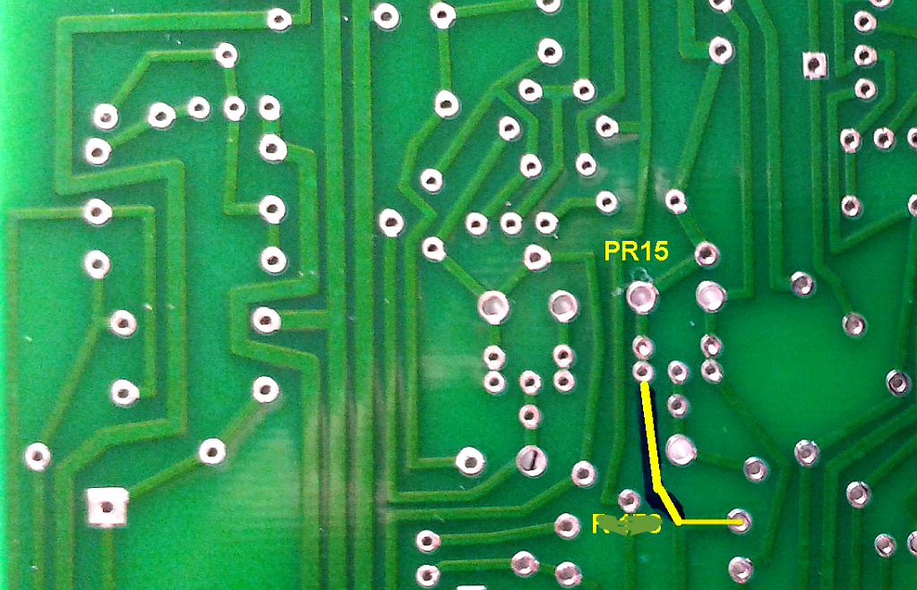
Oscillator 1
The first operation is to adjust the shape of thesinewave, since the adjustment affects frequency. Using the vernier control and PR15 if necessary, obtain an output of 400Hz. Turn the ramp down and adjust the sine shape control for the best sine shape.Trim PR17 to balance out the spike on the peak of thesinewave. This may best be seen by expanding the X and Y inputs on the scope.
The best position is where the small spike is triangular and balanced. A small thin spike may also appear but is not important.
Test the main shape control. A good sine wave should be achieved on 5.Set PR16 halfway and leave it alone. Set frequency vernier dial to 6
(±% division). If further out, R197 or R201 may need to be adjusted.
and adjust PR15 for 261Hz. Rotate vernier to 8 and check for 2088Hz.
Absolute maximum error ± 1 division. For fudge procedure, see Osc 2write up.
Sine Output should be around 1.5V p.p RampOutput should be around 1.5V p.p
N.B. Ramp shape is not controllable. Pitch characteristic is 0.32 Volts/Octave.
Oscillator 2
Set square level to zero, ramp at maximum. Set PR20 halfway. Vernier on 6.
Trim PR19 for 261Hz. Increase vernier to 8. Check frequency is about 2088Hz. If beyond spec then R291 SOT will have to be added in the range 8-22K.
Check that 10 on vernier dial gives at least 10kHz.
If vernier dial at 8 gives less than 2088Hz then short circuit R291 and R213
will have to be reduced. These should be 2% resistors.
Shape controls should operate identically to those on Osc. 3 (see next page) except that levels are reduced, and the two outputs are summed into the
patchboard on Mark II machines. Remember to turn down unwanted signal. Resistors R226 and R228 are the relevant ones to set the shape. Pulse level should be 2V p.p. Ramp level should be 3.5V.
N.B. Osc.2 and 3 waveforms are not symmetrical with respect to zero volts.
Tracking
Mix Osc. 1 and Osc. 2 ramp outputs into Output Channel 1. Use PR20 only to trim the tracking of Osc. 1 and Osc 2. Using the joystick on max with range control to limit frequency range. Set both verniers to 6 and tune for zero beats. Advance the joystick range control, which will increase both frequencies until the beats begin. Trim PR20 to zero beats, and remember which way you turned it. (N.B. The preset is a very fine adjustment, and when the tracking is nearly right it will be necessary to make very very small movements). Having trimmed PR20, turn the range control back to zero, re- adjust one of the verniers near 6 to give zero beats and then advance range control of joystick to where it was before. If beats are faster you know you turned the preset the wrong way. Repeat procedure until tracking goes to about 2kHz. Ideally a test 'back’ should now be fitted and a final adjustment made after another 10 minutes have elapsed.
Faults
Tracking from 261Hz to about 2kHz should be achieved with a maximum of 3 beats per second all the way. A curved Voltage/Frequency response may occur where zero beats are produced in more than one place. This is due to a mismatch in the matched pair transistors (Q74 and Q75 for Osc. 2). Fit a new transistor here or in Osc. 1.
N.B. Always use specially matched 2K7 pins for tracking tests.
Oscillator 3
Check frequency control pot for even change in frequency.
Adjust PR21 so that when the vernier is at 8 the frequency is 63Hz.
Note: Vernier 10 should give 5OOHz. Period at 0 should be greater than 20 sec.Adjust values of R261 & R262 with pad resistors to achieve correct shapes
of waveforms as shown below:
Triangle and square wave should occur on 5. Maximum of % division error
allowed. Check Voltage control input.
Faults Osc. 3 breaks through to Osc. 2 and to a lesser extent Osc. 1. Effect dependent on Osc. 3 shape control setting. Triangle was ‘furry’, with lOmHz oscillations
visible all over ‘C’ board. Strongest near Q101. Cause: instability in Q99.Q100, Q101. Cure, C70 330pF change to 1nF.
Click to expand
Noise and Meter
Noise Generator
Set the Colour control on 5, max output. Select a transistor which gives wideband noise and can be adjusted to give 3V p.p with PR22 roughly midway (to give some later adjustment margin). Lumpy or crackly sounding transistors should be rejected.
Meter
Check left hand zero of meter with machine off or switched to Signals. Move the switch to Control Voltages position and adjust PR14 for accurate centre zero. Switch the meter switch a few times and recheck zero again. Patch the joystick to Meter for swings in both + and — directions.
Check for needle sticking at either end of travel. Switch to Signalsand test with Osc 2 sawtooth at max level. Vary level to check
proportionality.
Faults
Meter: R174 and R173 are swapped
check the Germanium Diode on bottom
Calibration (from Hinton)
click to expand: (not preferred)
SOT = select on Test or use a trimmer
1. Check Mains voltage setting. 2. Plug in Card A only. 3. PSU Switch on. Adjust PR2 for +12 volts. 4. PSU Adjust PR1 for -9 volts. 5. Plug in Cards B and C. 6. PSU Recheck +12V and -9V. 7. REVERB Adjust Pr3 so that mixing occurs above 2 on the Reverb Mix knob. 8. REVERB Check the voltage control of reverb mix. 9. O/P Adjust PR4 and PR5 for zero residual signals. 10. O/P Check the tracking of Level knobs 4-5-6.
11. ENV Set Trapezoid speed to 65Hz with PR12 12. ENV Set PR13 clockwise. 13. ENV Adjust PR7 for minimum residual signal. 14. ENV Adjust PR13 until signal just reappears, then back off to zero. 15. ENV Check that maximum On time is at least 4 seconds. 16. ENV Check that maximum Decay time is at least 15 seconds. 17. ENV Check that recycling occurs with Off set at 5. 18. ENV Check that recycling does NOT occur with Off set above 7. 19. ENV Check that Trigger functions and does not jam.
20. FILT With filter in oscillation and Frequency control on 5, set PR6 for 261Hz. 21. FILT Check that Response control gives filtering below 5 and oscillation above. 22. FILT Check the shape of the oscillating Sine wave.
23. RM Adjust PR10 for fundamental rejection on A residual signal. 24. RM Adjust PR9 for 1st harmonic rejection on A residual signal. 25. RM Adjust PR11 for fundamental rejection on B residual signal. 26. RM Adjust PR8 for 1st harmonic rejection on B residual signal. 27. RM Check for frequency doubling when both inputs are the same.
28. I/P Check both channels for correct gain on both Hi and Lo inputs.
29. OSC1 Adjust PR17 for best sine wave shape. 30. OSC1 With Frequency on 6 set PR15 for 261Hz. 31. OSC1 With Frequency on 8 add R290 (sot) to achieve 2088Hz. 32. OSC1 Recheck last two steps. 33. OSC1 Check both waveforms. 35. OSC2 Set PR20 half-way. 36. OSC2 Pad shape resistors R227/R228 to achieve correct shapes. 37. OSC2 With Frequency on 6 set PR19 for 261Hz. 38. OSC2 With Frequency on 8 add R291 (sot) to achieve 2088Hz. 39. OSC2 Recheck last two steps. 40. OSC1/2 Adjust PR20 to achieve oscillator tracking to 2kHz. 41. OSC3 Pad shape resistors R261/R262 to achieve correct shapes. 42. OSC3 With Frequency on 8 set PR21 for 63Hz.
43. NOISE Select a (transistor) diode for good bandwidth and level. 44. NOISE Adjust PR2 for around 3 volts p-p noise. 45. NOISE Check the operation of the noise colour control.
46. METER Set signal zero on the meter itself and check operation. 47. METER Adjust PR14 for control voltage zero.
48. JOYSTICK Adjust vertical for equal excursions on meter. 49. JOYSTICK Adjust horizontal for equal excursions on meter.
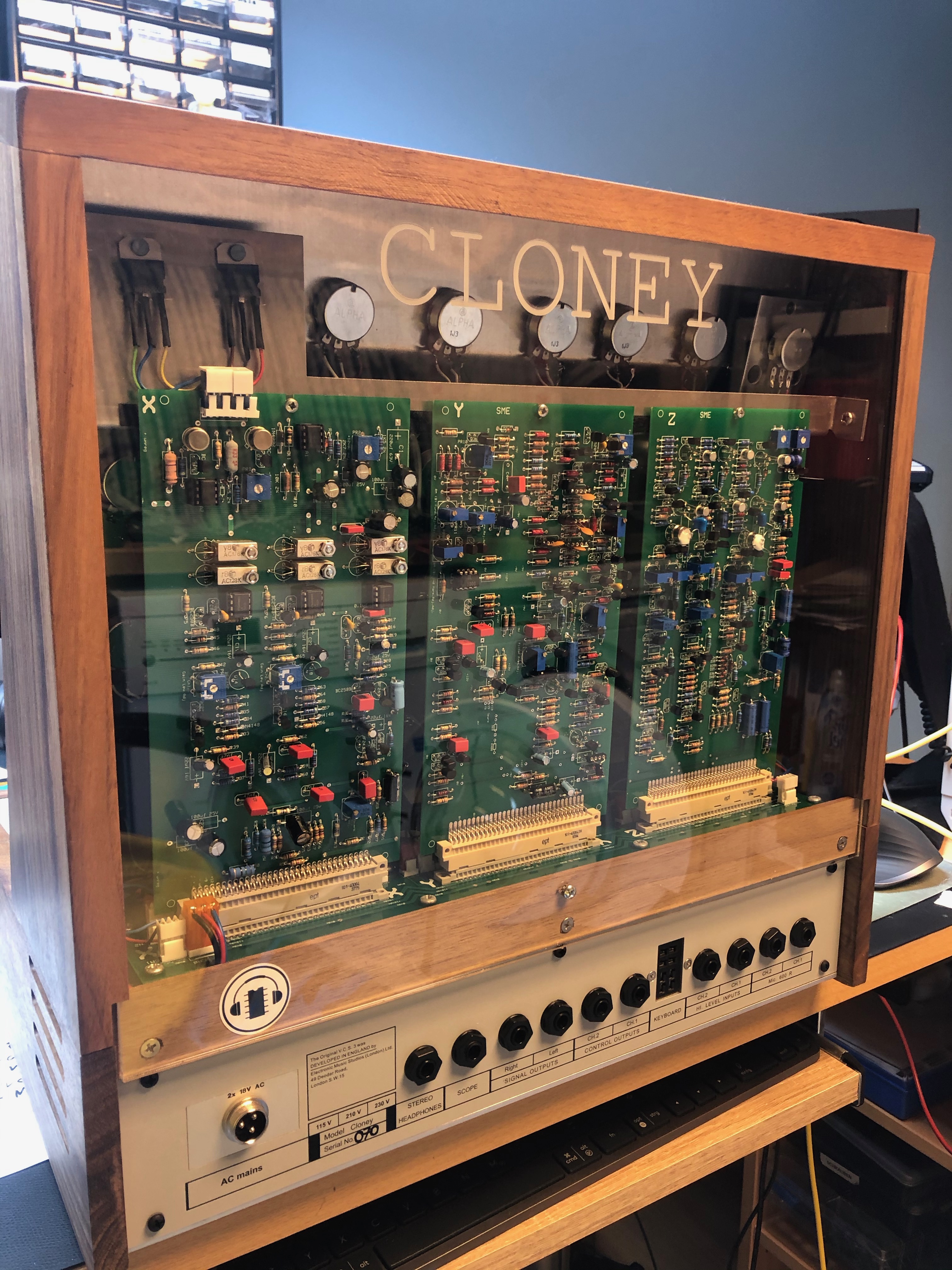
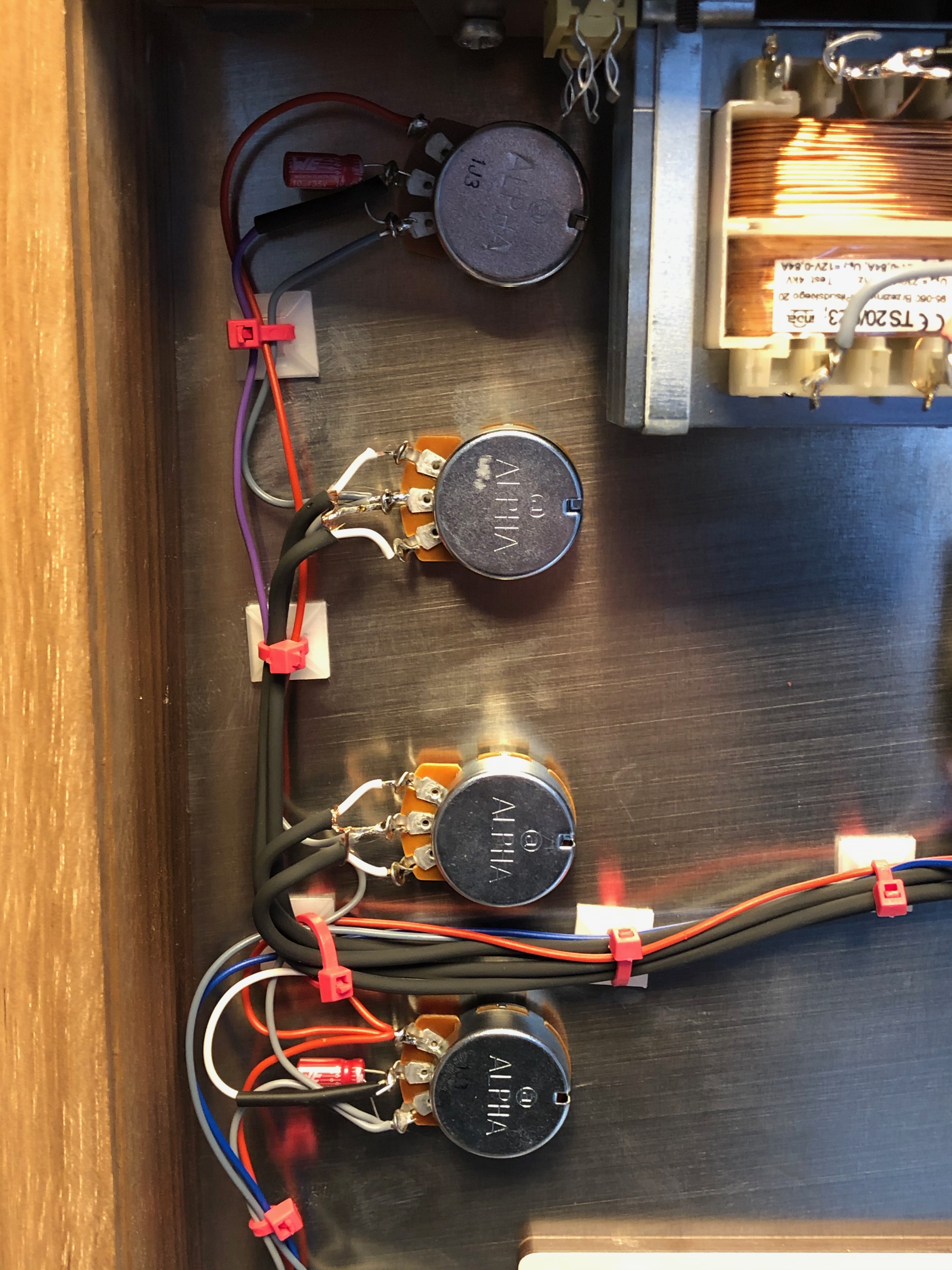
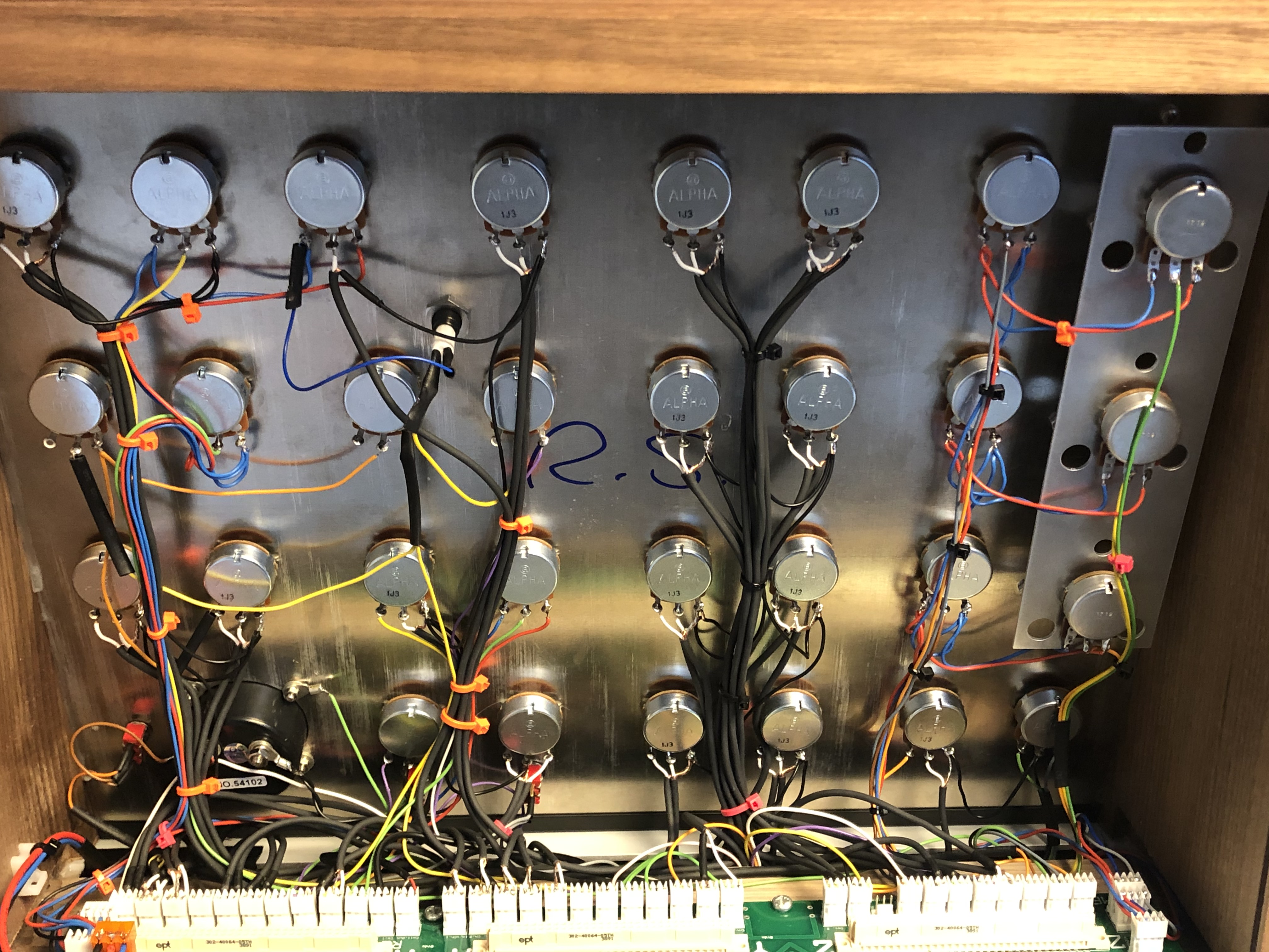
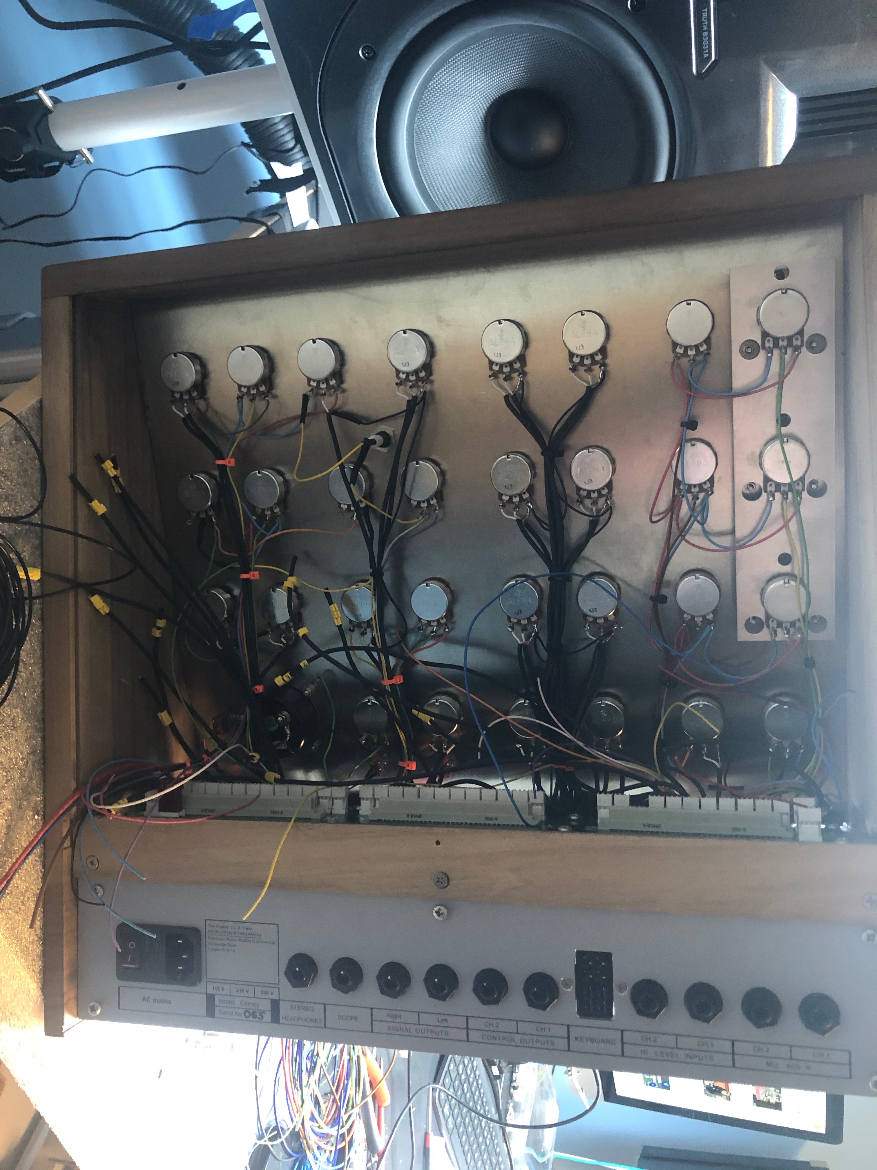
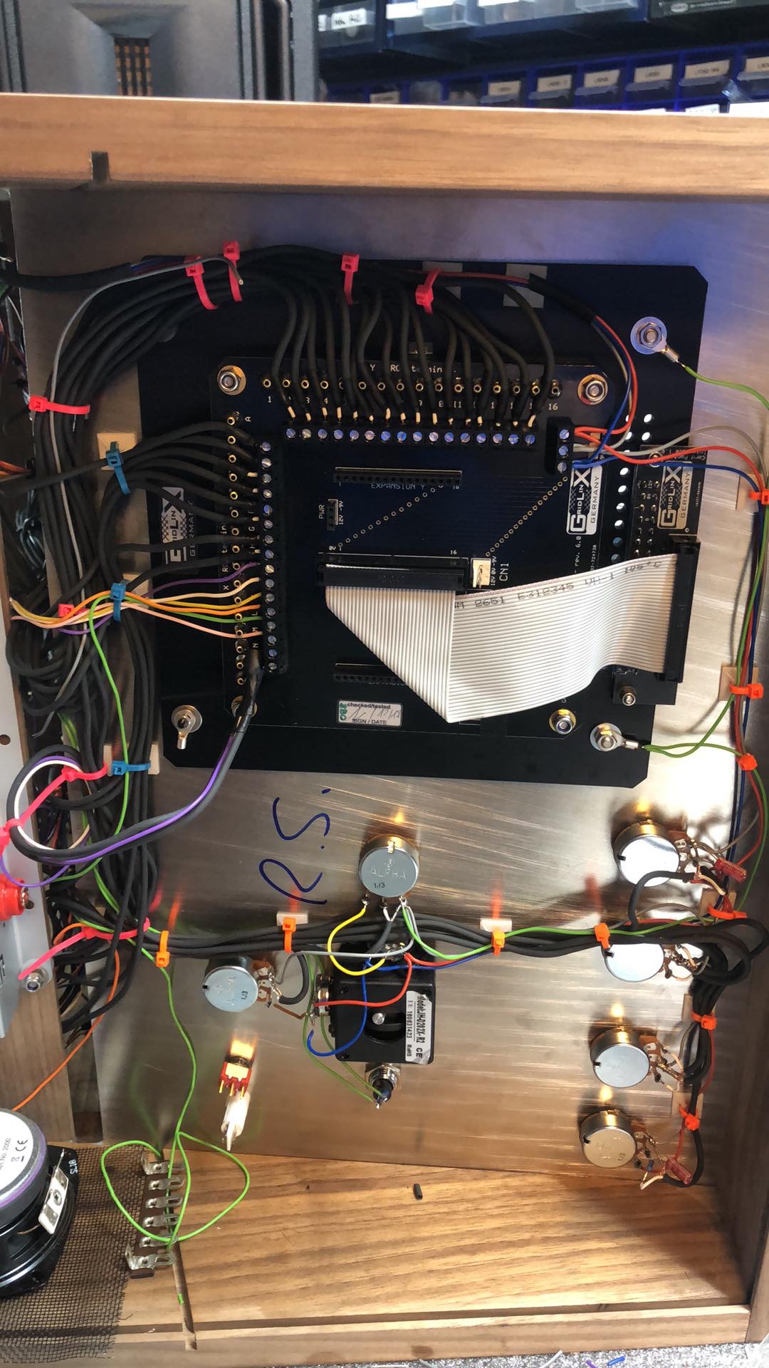
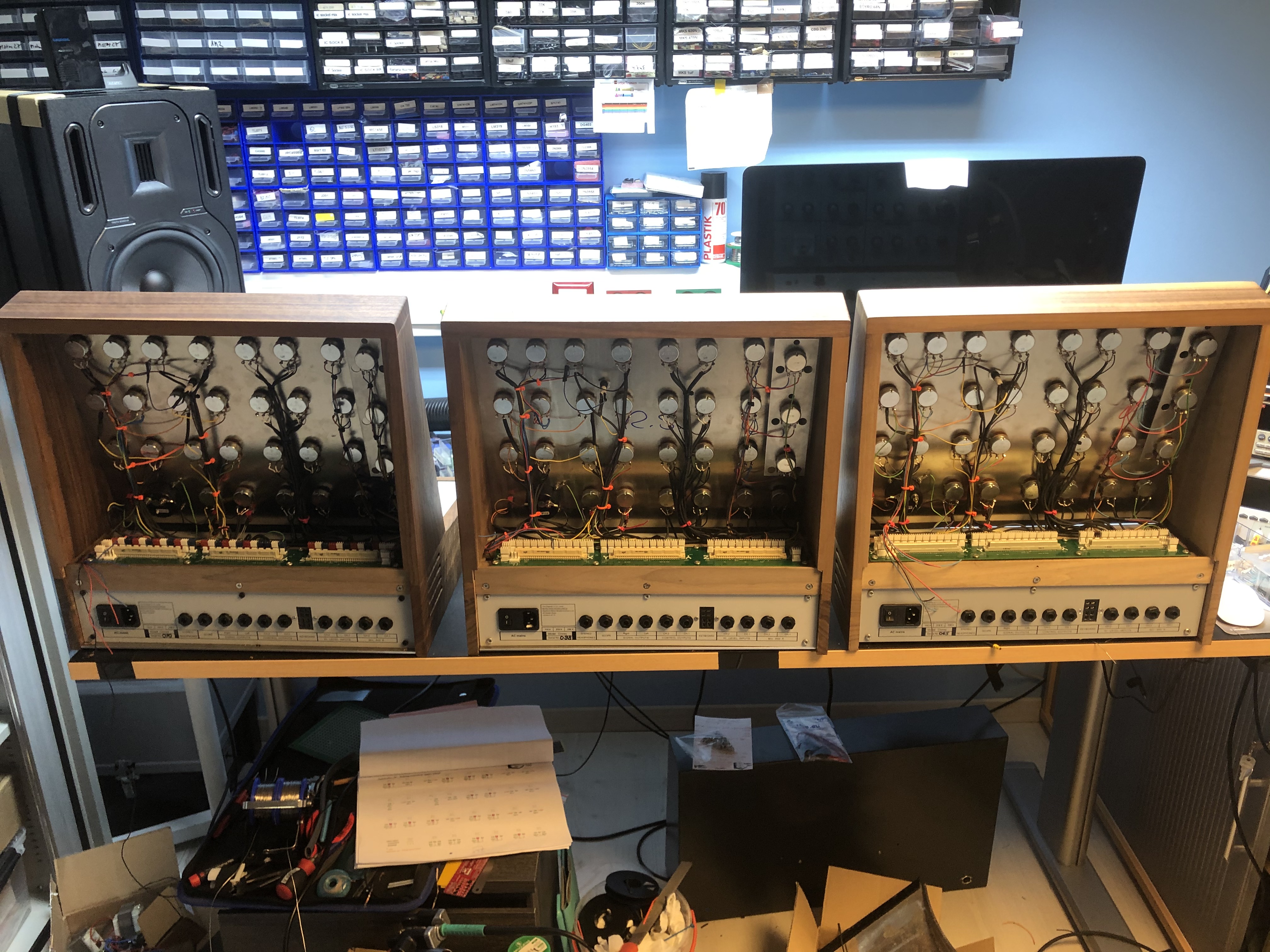
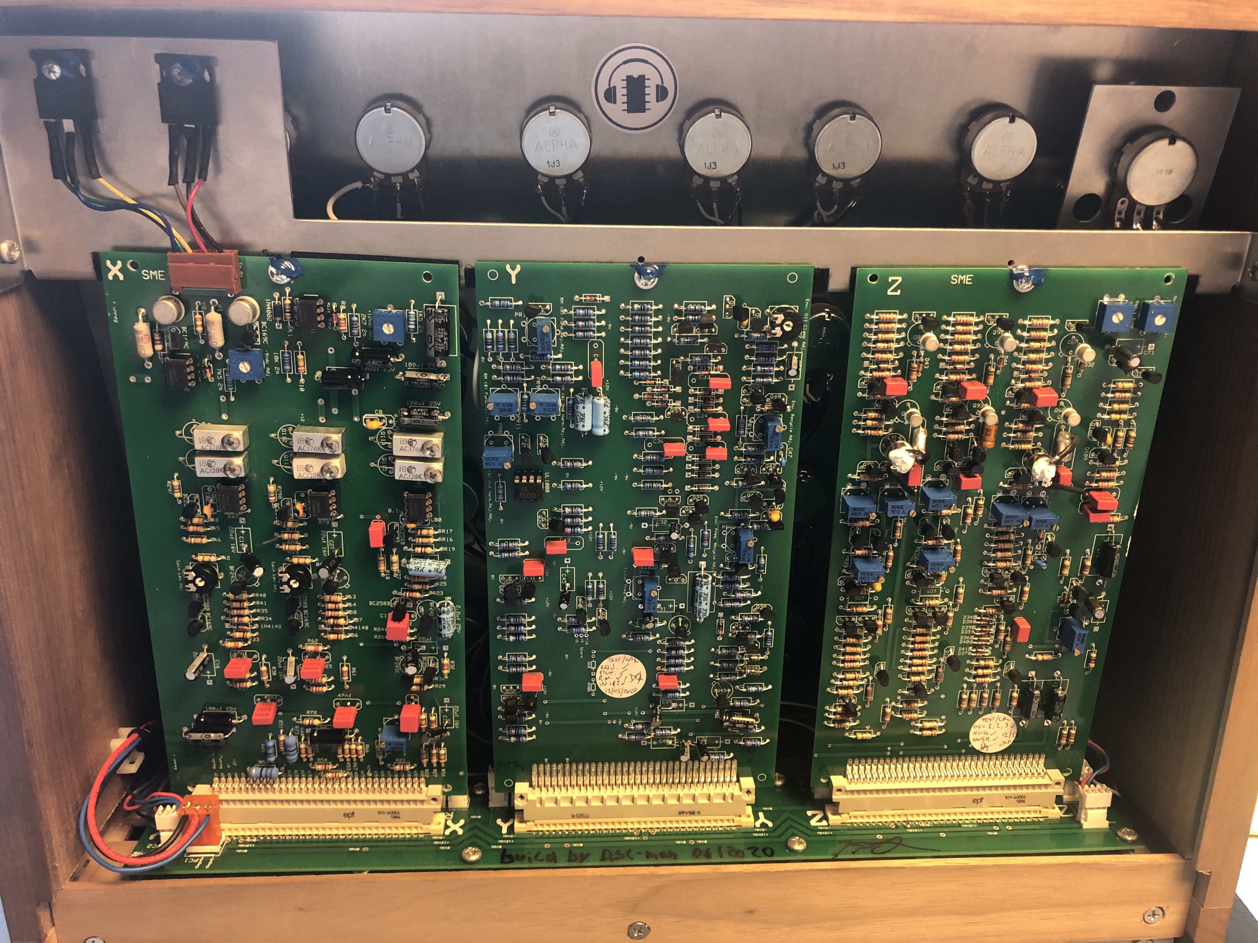
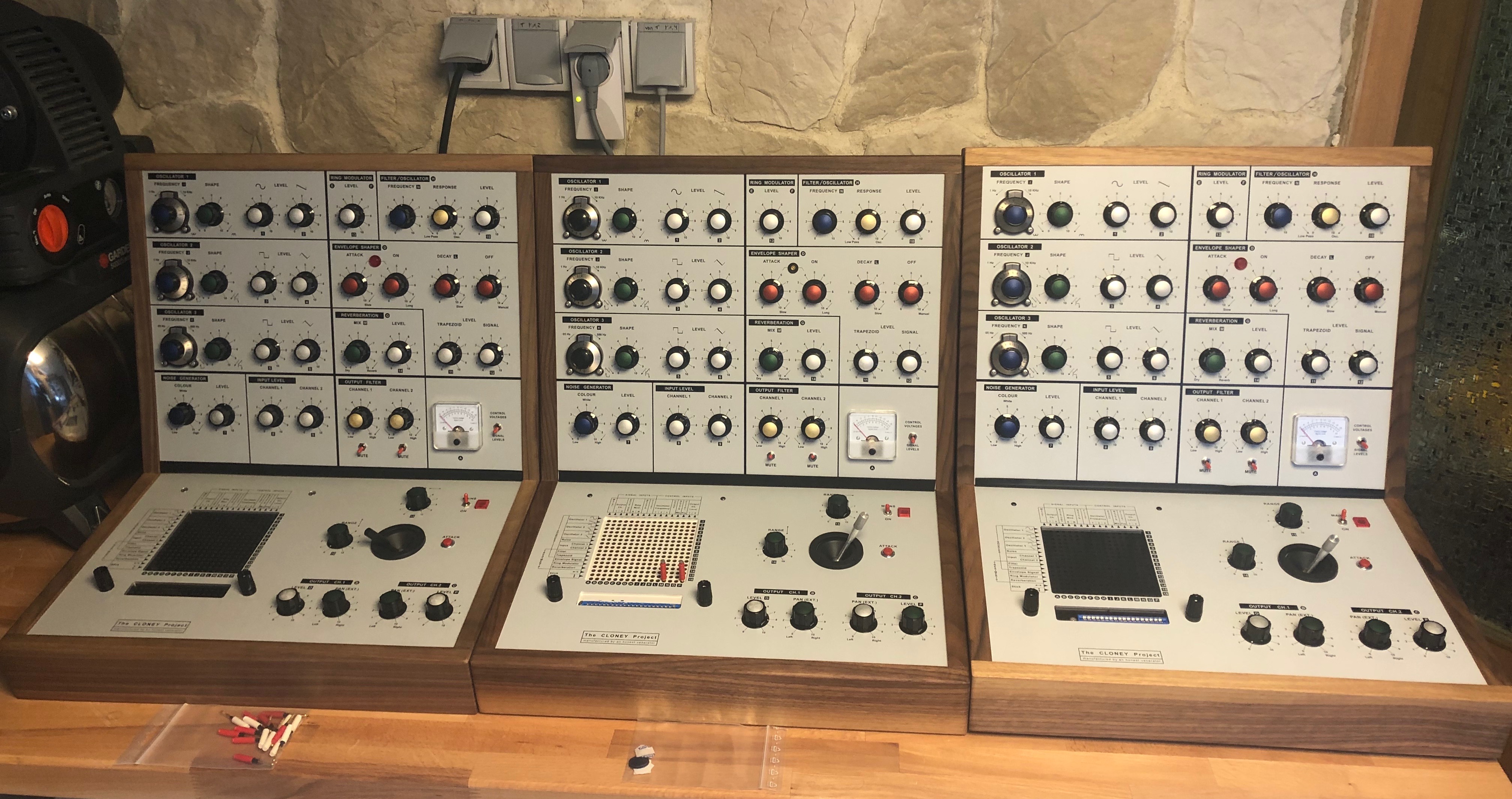
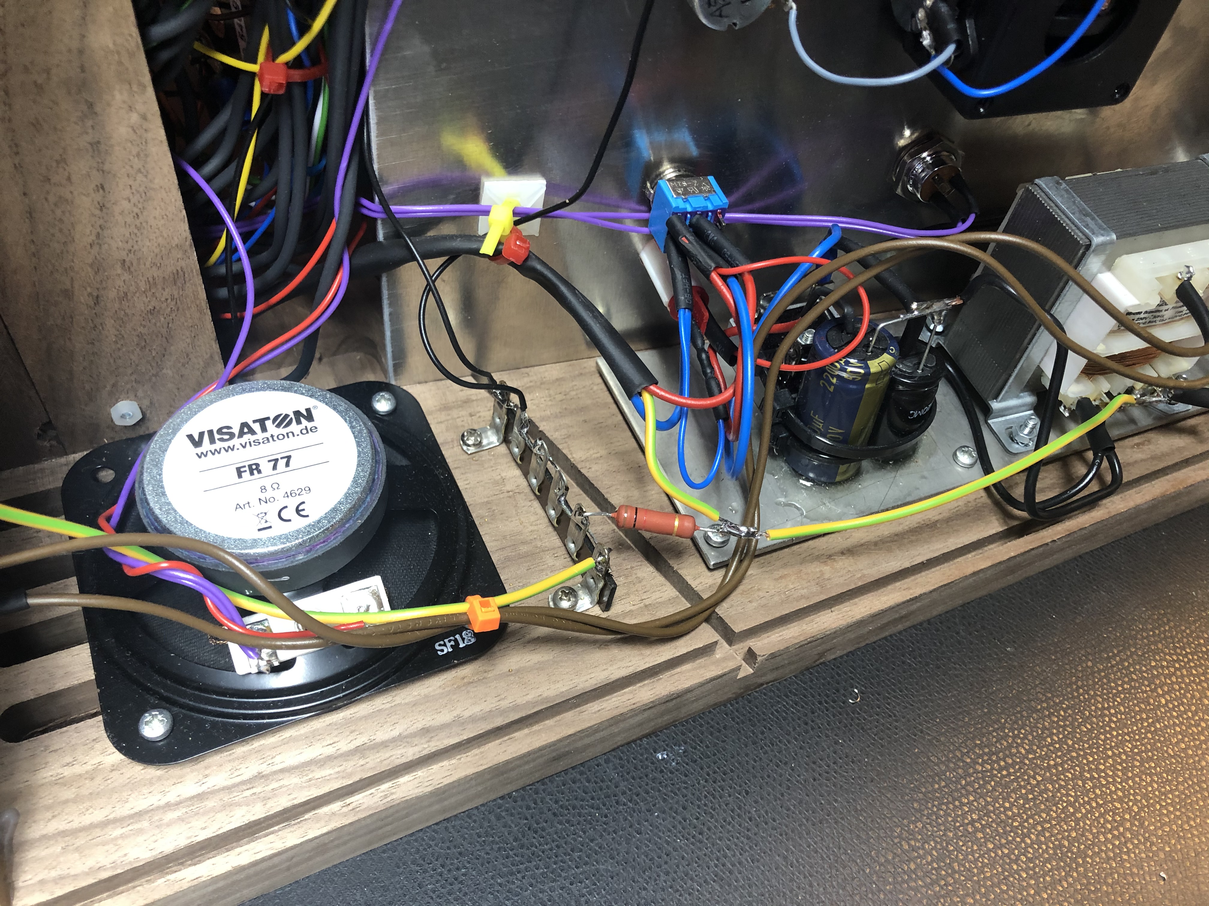
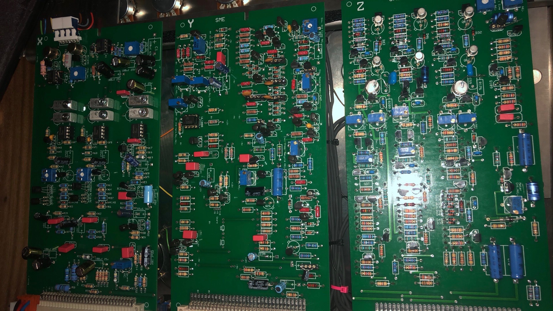
my own build tips, here are some pictures of my 5 builds: